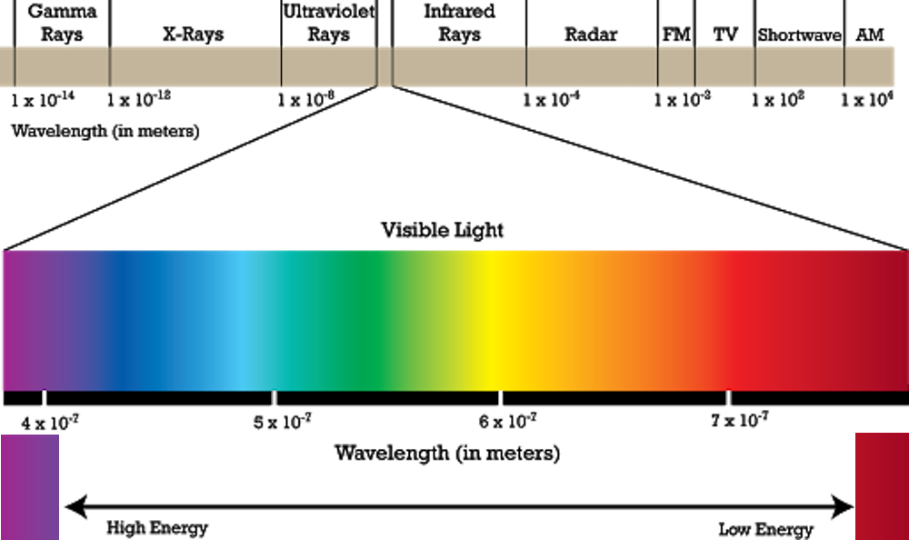


A normal microscope uses visible light (electromagnetic spectrum) that bounces off the specimen under the microscope to create images. There are many types of waves that make up the electromagnetic spectrum. Visible light is just a small part of it. Other types include X-rays, gamma rays etc. Since visible light is not exactly from the ‘smallest wavelength’ part of the electromagnetic spectrum, the bounced wavelengths aren’t very small themselves and cannot produce images of small specimens.
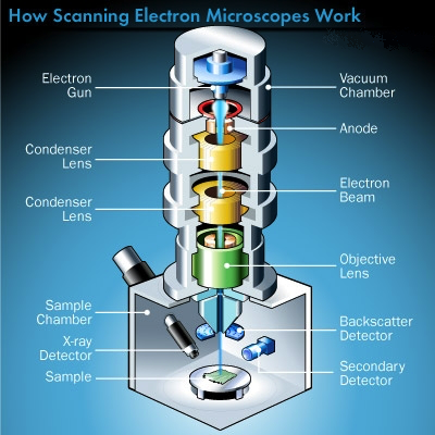
A Scanning Electro Microscope (SEM) use beams of electrons, instead of normal light, to image the specimen. Since electrons are way smaller than photons (visible light particles) they have a higher magnification power.
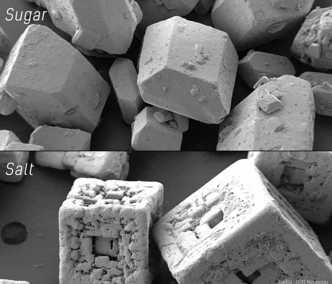
Scanning electron microscopes utilize a beam of focused electrons of relatively low energy as an electron probe that is scanned over the specimen. An electron beam source (cathode) and electromagnetic lenses generate and focus the beam. The electron beam stimulates emission of high-energy backscattered electrons and low-energy secondary electrons from the surface of the specimen. The sensor then builds an image of the surface of the specimen.
An optional X-ray detector also senses the backscatter of reflected energy in the X-Ray bandwidth of the spectrum and interprets these frequencies of the energy waves. This process yields a spectrographic analysis, that provides the operator with the chemical composition of the specimen.
In order to yield the best imaging results, the specimen should be electrically conductive. Conductivity can be enhanced by evaporating a film of metal, such as gold onto the specimen in a vacuum in a process called ‘sputter coating’.
In 1976, I worked for awhile for an engineering company called Eaton, Yale & Towne. They produced parts for automobile engines. I was engaged to be the technician in charge of maintaining and operating a Scanning Electron Microscope. It was a fascinating tool and it was a very interesting introduction to the world of the very small.
Would you like to share your thoughts?
Your email address will not be published. Required fields are marked *